Difference between revisions of "HANcoder/Training Material/MPU6500"
| Line 17: | Line 17: | ||
First, when the counter value is 0, register 0x6A and 0x6B are written. The next register, 0x68, is written when the counter value is 11 which is a delay of 110ms. After all the configuration subsystems (green blocks) are executed, reading the sensor signals begins in the orange subsystem. Let's look inside one of the configuration subsystems:<br/> | First, when the counter value is 0, register 0x6A and 0x6B are written. The next register, 0x68, is written when the counter value is 11 which is a delay of 110ms. After all the configuration subsystems (green blocks) are executed, reading the sensor signals begins in the orange subsystem. Let's look inside one of the configuration subsystems:<br/> | ||
[[File:MPU6500_SPIconfigSubsystem.png|400px]]<br/> | [[File:MPU6500_SPIconfigSubsystem.png|400px]]<br/> | ||
| − | Here two registers are written using 4 transfers of a byte. The first bit of the first byte indicates if it is a read (1) or a write (0) action. The following 7 bits are the address bits of the register. After this the value can be send to the MPU6500. A value of 0x9F is send, this means: I2C disable, FIFO disable, FIFO reset, etc. Immediately after the next register is written. SPI works with a slave select pin, this pin is pulled low before the transfer so the slave knows the data is for him. The slave select pin is kept low until the data to the second | + | Here two registers are written using 4 transfers of a byte. The first bit of the first byte indicates if it is a read (1) or a write (0) action. The following 7 bits are the address bits of the register. After this the value can be send to the MPU6500. A value of 0x9F is send, this means: I2C disable, FIFO disable, FIFO reset, etc. Immediately after the next register is written. SPI works with a slave select pin, this pin is pulled low before the transfer so the slave knows the data is for him. The slave select pin is kept low until the data to the second byte has been successfully send. The screenshot below is the mask with the settings for the transfer of the first byte. It can be seen that the slave select pin, pin D7 is enabled 50 delay cycles before transfer.<br/> |
[[File:MPU6500_SPIconfigTransferSettings.png|400px]]<br/> | [[File:MPU6500_SPIconfigTransferSettings.png|400px]]<br/> | ||
| + | After the second byte, with data, has been transferred the slave select pin is disabled. The same procedure is followed while transferring the address and data of register 0x6B. | ||
| + | In Simulink the position of the blocks in the model doesn't ensure the execution order of the blocks, it could be that the byte transfer which is on the top of the model is executed as last. To ensure the sequence of byte transfers is correct you can use priorities. Right-click the (HANcoder) block and choose 'Properties', in this screen the priority can be entered. Priority 1 will be executed before a block with priority 2.<br/> | ||
| + | [[File:MPU6500_SPIconfigTransferPrio.png|400px]] | ||
Revision as of 12:13, 6 April 2017
Contents
MPU6500 3 Axis gyro and 3 axis accelerometer
The MPU6500 has a programmable scale for both the gyroscope and the accelerometer. It can measure angular rates up to 2000°/sec and up to 16G of acceleration. The sensor can be configured and read by using the SPI bus.
Connecting the MPU6500
First the MPU6500 must be soldered on the prototype PCB. It is wise to solder some female headers onto the PCB and male headers onto the MPU6500 so it can be replaced when broken. Make sure it is mounted ruggedly to make sure the sensor won't measure movements of the sensor relative to the board. Next the pins must be connected to the E407 pins, see the connection diagram below.
SPI control in Simulink
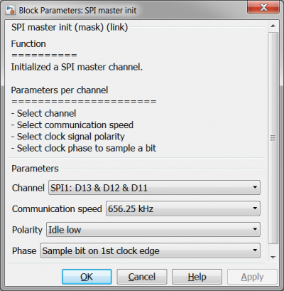
As mentioned before the communication with the sensor is done via SPI. First the SPI Master Init block is used to initialize the SPI system. Channel 1 is chosen with a baud rate of 656.25kHz because the datasheet states that the maximum SPI clock frequency is 1Mhz. The polarity is chosen to be 'Idle low' and phase 'Sample bit on 1st clock edge', these settings also come from the datasheet of the MPU6500.

Configuring the MPU6500
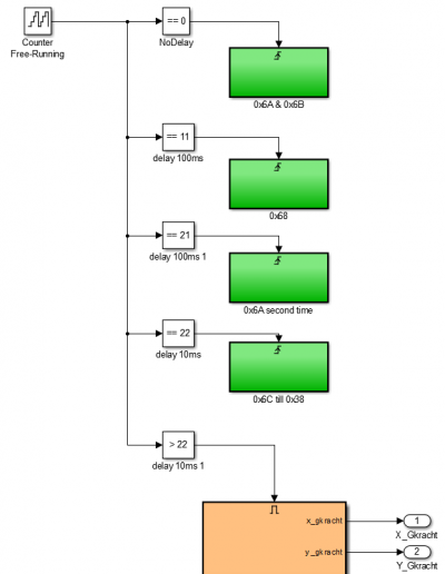
The MPU6500 needs to be configured, because the chip needs some time to process the configurations some delay has to be added between sending the bytes. This is done with the use of a free running counter. The counter increases every 10ms so by checking the output of the counter a delay can be generated. See the Simulink model screenshot below:

First, when the counter value is 0, register 0x6A and 0x6B are written. The next register, 0x68, is written when the counter value is 11 which is a delay of 110ms. After all the configuration subsystems (green blocks) are executed, reading the sensor signals begins in the orange subsystem. Let's look inside one of the configuration subsystems:
![]()
Here two registers are written using 4 transfers of a byte. The first bit of the first byte indicates if it is a read (1) or a write (0) action. The following 7 bits are the address bits of the register. After this the value can be send to the MPU6500. A value of 0x9F is send, this means: I2C disable, FIFO disable, FIFO reset, etc. Immediately after the next register is written. SPI works with a slave select pin, this pin is pulled low before the transfer so the slave knows the data is for him. The slave select pin is kept low until the data to the second byte has been successfully send. The screenshot below is the mask with the settings for the transfer of the first byte. It can be seen that the slave select pin, pin D7 is enabled 50 delay cycles before transfer.
![]()
After the second byte, with data, has been transferred the slave select pin is disabled. The same procedure is followed while transferring the address and data of register 0x6B.
In Simulink the position of the blocks in the model doesn't ensure the execution order of the blocks, it could be that the byte transfer which is on the top of the model is executed as last. To ensure the sequence of byte transfers is correct you can use priorities. Right-click the (HANcoder) block and choose 'Properties', in this screen the priority can be entered. Priority 1 will be executed before a block with priority 2.
![]()